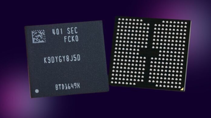
Samsung 9th generation V-NAND
In order to maintain its dominant position in the NAND flash market, Samsung Electronics, the global leader in advanced memory technology, today announced that mass production of its one-terabit (Tb) triple-level cell (TLC) The First 9th-Gen V-NAND (vertical NAND) has started.
Creating the First 3-D Vertical Structure Era
The duration of the human species is remarkably less than 14 seconds, if the history of the universe is considered a single year. The Sun and Earth are by no means at the centre of the universe’s development, as there are more than 170 billion known galaxies that are continuously expanding. Semiconductors can be compared in this same way.
A miniature universe can be observed by using an electron microscope to examine a semiconductor chip that is smaller than the size of a fingernail. In order to store enormous amounts of data, a chip with a thickness of only 1mm has millions of precisely designed spaces inside of it.
For many years, data-storing NAND flash memory solutions had a two-dimensional (2D) architecture in which chips were stacked and placed on flat surfaces. However, the amount of data that could be stored in these 2D structures was severely constrained.
Following a great deal of research to address this problem, Samsung invented V-NAND (vertical memory, where the “V” stands for vertical) flash memory, a technology that joins its cell layers via perforations in 3D space that is stacked vertically. The world’s first company to design and market a memory solution of this kind is Samsung.
This 3D V-NAND entered the market , revolutionising memory semiconductors from the 2D structure that had dominated electronic storage for decades. It permitted technical transition similar to people moving from 1- or 2-story residences to high-rise flats for the first time.
Samsung’s Semiconductor Solution Victory: V-NAND
Since its groundbreaking introduction, the V-NAND solution which features a revolutionary vertical 3D structure has become the industry standard.
When Samsung first developed a V-NAND solution in 2013, it had 24 layers; that number has grown to nearly 200. But just piling more layers on top of one another isn’t enough, much like in high-rise apartments.
As a building’s height increases, an apartment should be both tall and sturdy, with easy access via a reliable lift. Furthermore, a building’s height is limited by altitude constraints, and noise levels between floors need to be taken into account.
Regarding the V-NAND solution, the same holds true. Small variations in functionality and structure can be seen even in cases where the number of layers is comparable. This can be crucial in the semiconductor industry because even the smallest variation can have a profoundly different effect.
9th-Gen V-NAND
Bit density that leads the industry, up roughly 50% from the previous generation. The revolutionary double-stack structure of the V-NAND enhances productivity with cutting-edge “channel hole etching” technology.
“Samsung is thrilled to offer the first 9th-gen V-NAND to the industry, which will significantly advance future applications. Samsung has pushed the envelope in cell architecture and operational scheme for their next-generation product to meet the changing needs for NAND flash solutions, according to SungHoi Hur, Head of Flash Product & Technology of Samsung Electronics’ Memory Business. “Samsung will continue to set the trend for the high-performance, high-density solid-state drive (SSD) market that meets the needs for the coming AI generation with their latest V-NAND.”
Samsung increased the bit density of the Samsung 9th generation V-NAND by roughly 50% over the 8th-generation V-NAND, using the thinnest mould and the smallest cell size in the industry. The quality and dependability of the product have been improved by the application of new technologies such cell interference avoidance and cell life extension, while the planar area of the memory cells has been greatly decreased by the removal of dummy channel holes.
Furthermore, Samsung demonstrates its leadership in process capabilities with its cutting-edge “channel hole etching” technology. By stacking mould layers, this technique generates electron pathways and increases fabrication productivity by allowing the industry’s highest cell layer count to be simultaneously drilled in a double-stack structure. More complex etching techniques are needed to penetrate through higher cell numbers as the number of cell layers rises.
With “Toggle 5.1,” the next-generation NAND flash interface, the 9th-gen V-NAND can handle data input/output speeds up to 3.2 gigabits per second (Gbps), a 33% increase over its previous generation. By adding more PCIe 5.0 support along with this new interface, Samsung hopes to bolster its position in the high-performance SSD market.
Thanks to developments in low-power design, power consumption has also improved by 10% over the previous generation. Samsung 9th generation V-NAND is anticipated to be the best option for upcoming applications as consumers’ need to reduce energy use and carbon emissions grows.
Samsung began mass producing the 1Tb TLC Samsung 9th generation V-NAND this month, and in the second half of this year, it will launch the quad-level cell (QLC) model.
Samsung 9th generation V-NAND Specs
| Specification | Detail |
|---|---|
| Layers | 290+ |
| Structure | Double-Stacked |
| Interface | Toggle 5.1 |
| Data Transfer Speed | Up to 3.2 Gbps (33% increase over previous gen) |
| Status | In Mass Production |

