V-NAND Technology Upgrade
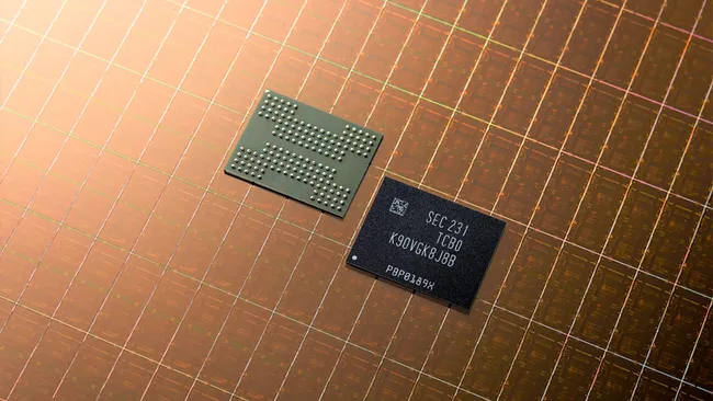
As the business that produces the most NAND memory chips in the world, Samsung has ambitious goals for the development of its V-NAND, which is what the company refers to as its 3D NAND. Some of these ambitions were shared with the public this week. The business has stated that its 9th Generation V-NAND memory would feature the largest number of active layers in the market and that it has confirmed that it is on schedule to develop its 9th Generation V-NAND memory with over 300 layers in the year 2024.
“The ninth-generation V-NAND is well under way for mass production early next year with the industry’s highest layer count based on a double-stack structure,” Jung-Bae Lee, President and Head of Memory Business at Samsung Electronics, said in a blog post. “The ninth-generation V-NAND is well under way for mass production early next year with the industry’s highest layer count based on a double-stack structure.”
In August, we found out that Samsung was hard at work on the 9th Generation of V-NAND, which would have over 300 layers and will continue to use the double-stacking technique that Samsung used for the first time in 2020. Not only did Samsung affirm that it is on track with the development of its next-generation non-volatile memory, but it also stated that it will supposedly feature more active layers than the 3D NAND memory produced by Samsung’s competitors. Since we already know that the next generation of 3D NAND from SK Hynix will have 321 active layers, it would imply that Samsung anticipates that their memory will have even more.

Samsung will be able to boost the storage density of its 3D NAND devices because to the increased number of layers it has implemented. The business anticipates that future varieties of flash memory will not only improve in terms of storage density but also in terms of performance.
“Samsung is also working on the next generation of value-creating technologies, including a new structure that maximizes V-NAND’s input/output (I/O) speed,” according to Jung-Bae Lee.
Even though we do not know what kind of performance we can anticipate from Samsung’s 9th Generation V-NAND, we can be certain that the company will employ this memory for its next solid-state drives (SSDs). It is possible that this is when we will see the company’s retail SSDs with a PCIe Gen5 interface. These SSDs will be the successors of Samsung’s 990 Pro series, which are now among the top SSDs on the market.
In terms of technological innovation aimed at the longer term, Samsung is committed to achieving the lowest cell sizes in the industry by eliminating cell interference, lowering height, and maximizing the number of vertical layers. These goals will allow Samsung to achieve the smallest cell sizes in the industry. These advancements will play a significant role in pushing Samsung’s aim of building 3D NAND with over 1000 layers as well as highly differentiated memory solutions, and in ensuring that the company’s products and services continue to be relevant for datacenters, personal computers, and other applications.

[…] Samsung Intros 9.8 Gbps HBM3E “Shinebolt”, 32 Gbps GDDR7, 7.5 Gbps LPDDR5x Cam2 Memory […]