After summarising conventional package assembly, this article will be the first of two on wafer-level packaging, the other main semiconductor packaging type. Photolithography, sputtering, electroplating, photoresist (PR) stripping, and metal etching—the five core WLP processes—will be covered.
Fully intact wafer packaging
WLP precedes wafer dicing. In fan-in and fan-out wafer-level chip scale packaging (WLCSP), the wafer is intact throughout the process. WLP includes redistribution layer (RDL), flip chip, and through-silicon via1 (TSV) packaging, even though only part of their operations are done before the wafer is diced. Electroplating metal and pattern vary by package2. They all package similarly, as shown below.
After testing, wafers are dielectrically coated as needed. Photolithography exposes the chip pad again after dielectric layer testing.
A metal layer is sputtered on the wafer3. This metal layer helps the electroplated metal layer adhere and blocks metal chemical growth by blocking diffusion. It transfers electrons during electroplating and applies photoresist to create a layer while photolithography designs.
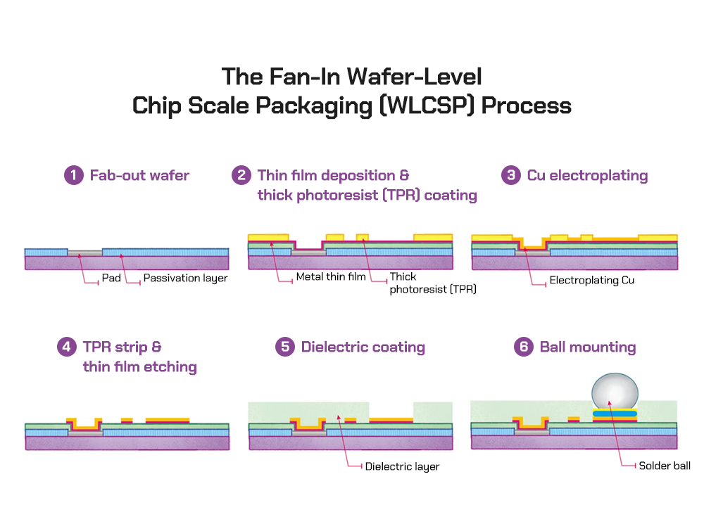
Electroplating coats metal thickly. After electroplating, PR stripping and etching remove thin metal layers. Wafers are electroplated with desired metal layers. This layout wires fan-in WLCSP, redistributes RDL pads, and bumps flip chip packaging. The following sections will examine each step.
Photolithography: Sketching Masked Wafer Pattern
Photolithography combines stone (litho) and drawing (graphy). Photolithography involves applying a photoresist to the wafer and selectively exposing it to light through a mask with a desired design. The light-exposed parts create the pattern. Process sequence is in Figure 2.
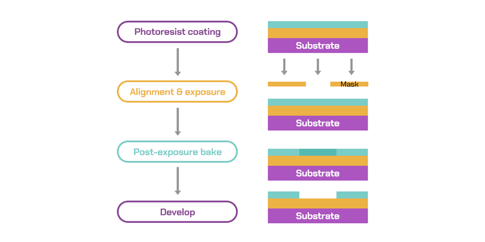
Photolithography is used in WLP to pattern dielectric, photoresist pattern electroplated, and etch diffusion layers for metal wiring.
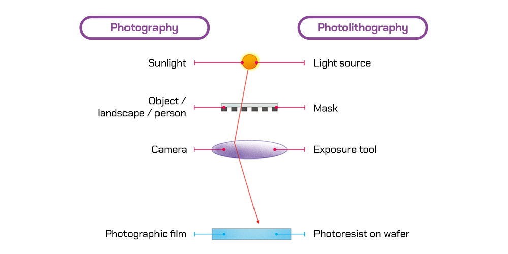
Compare photolithography to photography to understand it.
Figure 3 illustrates how sunlight photographs an object, scene, or person. Photolithography uses a light source to transfer mask designs to an exposure instrument. Finally, film in a camera is like photolithography wafer photoresist.
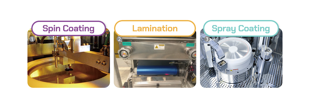
Figure 4 shows three wafer photoresist application methods. Spin coating, film laminating, and spray coating. Soft baking removes solvents after photoresist application to keep the viscous photoresist on the wafer and thick.
Spin coating spreads viscous photoresist from the centre of a spinning wafer to the edges due to centrifugal force (Figure 5). The wafer photoresist is uniformly thick. If spin speed is low and viscosity is high, photoresist is thick. Thinly apply if viscosity is low and spin speed is high.
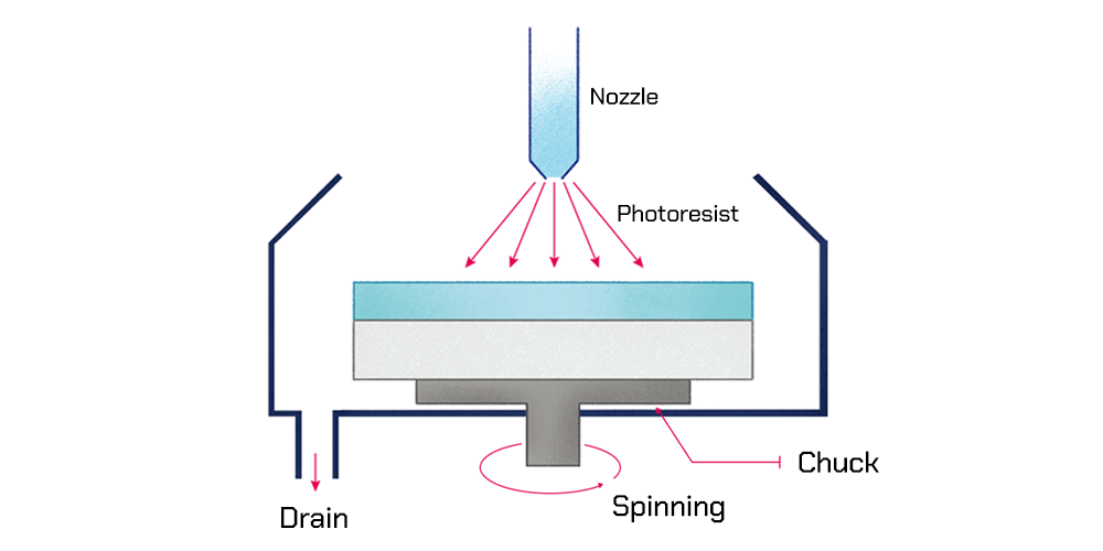
To generate solder bumps in wafer-level packages like flip chip, a photoresist layer of 30 to 100 μm thickness is required. Although a single spin coating is difficult to produce the right thickness. Some situations need lots of photoresist and soft baking. Lamination starts the film at the desired thickness, making it effective for thick photoresists. Processing without wafer waste is cheaper. However, rough wafer surfaces can hinder film adhesion, causing flaws. Spray coating uniformly thickens photoresist on rough wafers.
After coating and mild baking, photoresist is lit. The wafer’s photoresist receives the pattern from light through the mask. To remove a positive photoresist that weakens with light, the mask must have holes. A negative photoresist that hardens when exposed to light requires holes in the mask. Mask aligners4 or steppers5 are used for WLP photolithography.
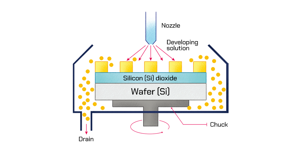
Developer solution dissolves photolithography-weakened photoresist. Figure 6 shows that puddle development pours the developer onto the wafer’s centre so it spins slowly, tank development immerses multiple wafers, and spray development sprays the developer. Figure 7 is a puddle chamber. After puddle development, photolithography patterns photoresist.
Films Sputtering: Wafer Thin
By physical vapour deposition6, sputtering creates a thin metal sheet on a wafer. Under bump metallurgy is the metal layer on flip chip wafers underneath the bumps. Two or three metal film layers consist of an adhesive layer, a current carrying layer that supplies electrons during electroplating, and a diffusion barrier with solder wettability7 to prevent compounds from forming between the plating layer and metal.
Titanium acts as the adhesion layer, copper as the current carrying layer, and nickel as the diffusion barrier. UBM affects flip chip package quality and dependability. Aramid and WLCSP metal wiring layers have adhesive and current-carrying layers to promote adhesion.
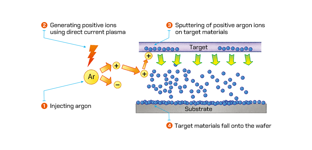
Argon gas becomes plasma8 and hits a target with the same composition as the metal on which positive argon ions will be deposited (Figure 8). Collisions deposit metal particles on the wafer from the target. The direction of metal particles in sputtering is constant. Trench or vertical connection access (via) plates can affect flat plates, even though they are uniformly thick. Uneven shapes can thin the wall’s parallel to metal deposition surface below the plate’s floor.
Bonding Metal Layers Electroplating
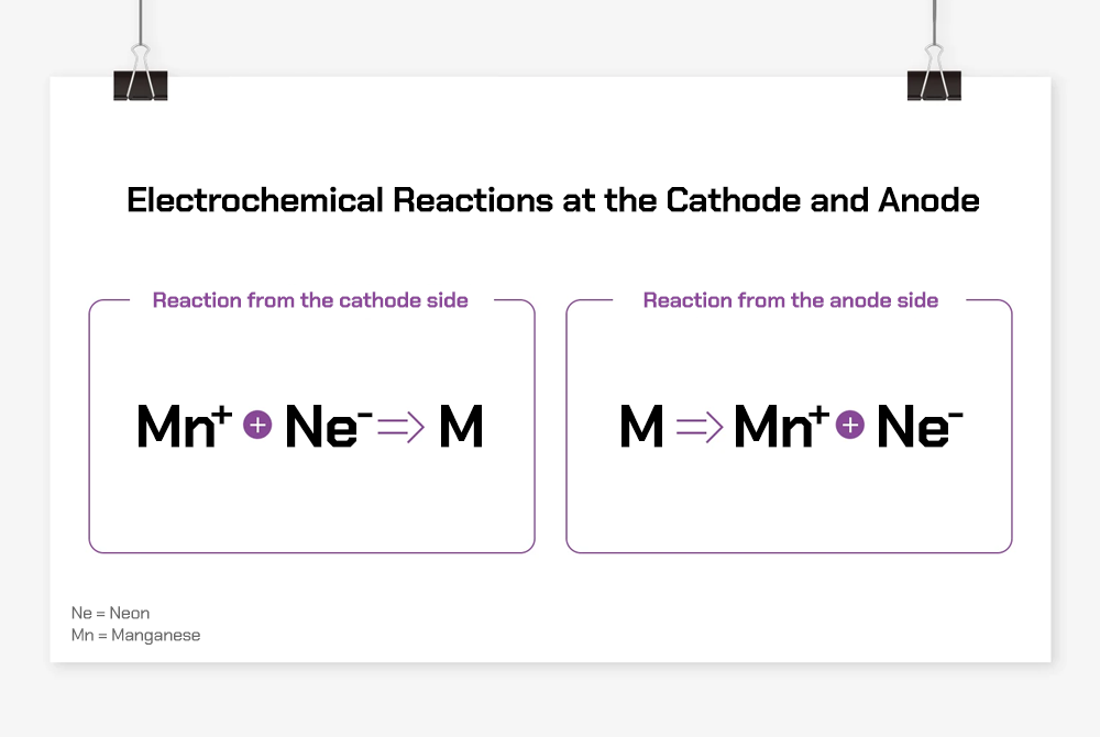
Electroplating deposits wafer metal ions from electrolyte solution. A reduction reaction with exogenous electrons does this. Electroplating coats WLP wire and electrical bumps with thick metal. Figure 9 shows how the anode oxidises a metal to create an ion and release electrons to the external circuit. Metal ions oxidised at the anode or in solution receive electrons and reduce to metal.
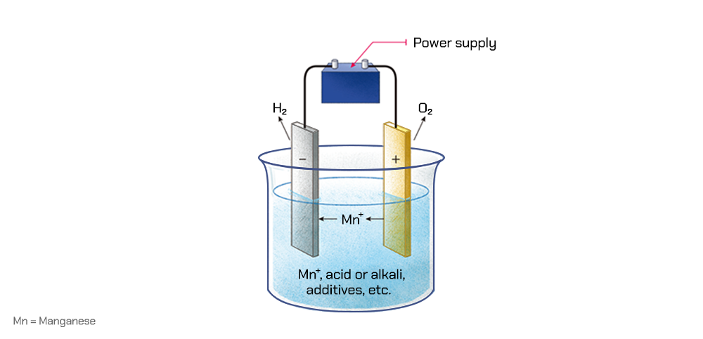
The cathode plate becomes a wafer with WLP electroplating. The anode plate uses an insoluble electrode like platinum and metal to be plated. Metal ions are dissolved and dispersed from the anode plate to maintain solution ion concentration. A wafer-plated insoluble electrode needs periodic metal ion replenishment to maintain ion concentration. The cathode and anode electrochemical reactions are shown in Figure 10.
The wafer’s side faces down and the anode is below the solution when electroplated. Solution flows towards the wafer and hits it hard, electroplating. Photoresist patterns on the wafer to be plated can now contact the solution. Electrons from electroplating equipment at the wafer’s edge encounter metal ions in the solution at patterned areas. Patterns mix with metal ions in the solution to reduce and create metal wiring or bumps.
Photoresist Removal: PR Stripping and Metal Etching
After using photoresist, PR stripping must remove it. PR stripping uses a chemical stripper to develop puddles, tanks, or sprays. The sputtering coating must be removed because electroplating creates metal wiring or lumps. The wafer will short circuit if the metal film is not removed. Acid-based wet etching dissolves metal coatings. As wafer metal patterns become finer, puddle development and PR stripping become more popular.


